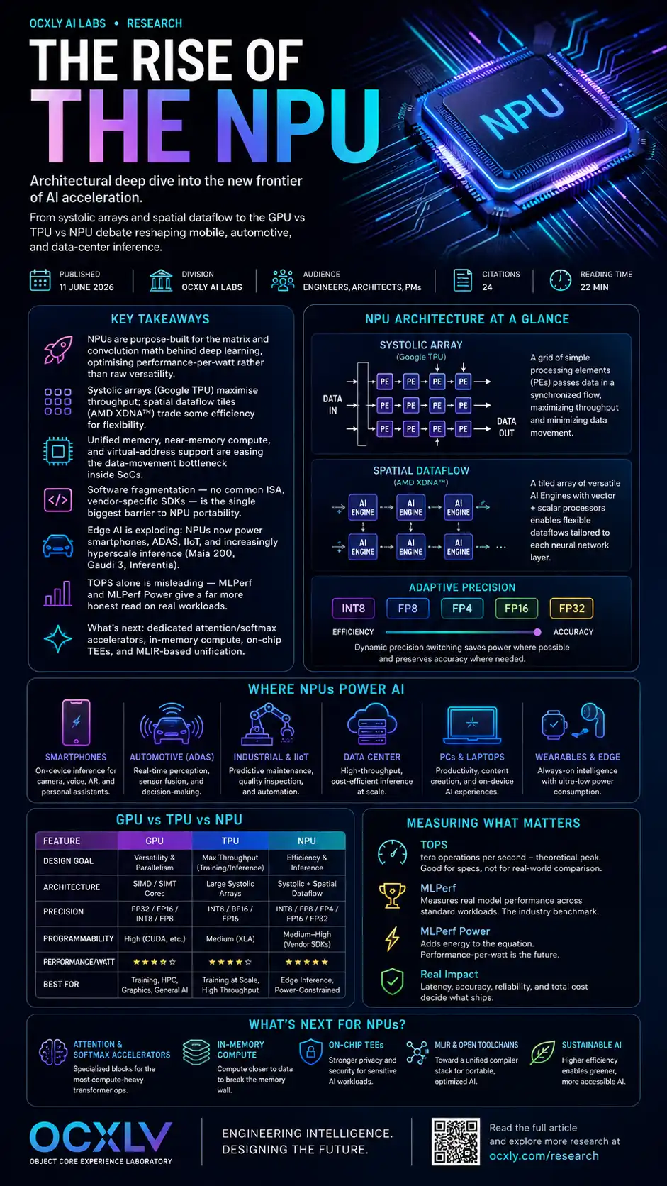
An architectural deep dive into the new frontier of AI acceleration — from systolic arrays and spatial dataflow to the GPU vs TPU vs NPU debate reshaping mobile, automotive, and data-center inference.
Published · 11 June 2026Division · OCXLY AI LabsAudience · Engineers, Architects, PMsCitations · 24
Reading mode
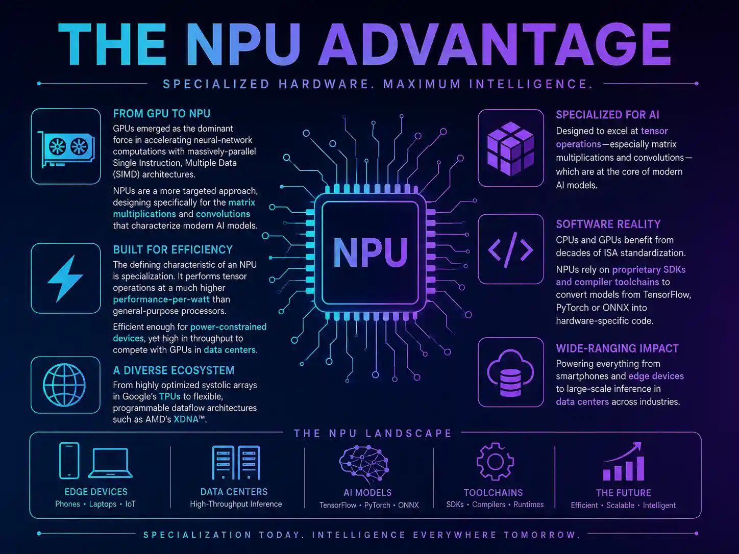
Neural Processing Units (NPUs) represent a specialised class of hardware accelerators designed to expedite the computationally intensive tasks inherent in artificial intelligence, particularly deep-learning models[1]. As AI workloads have grown in complexity and scale, the demand for efficient execution has driven innovation well beyond traditional CPUs.
While GPUs established themselves as the dominant force in accelerating neural-network computations through massively parallel Single Instruction, Multiple Data (SIMD) architectures, NPUs offer a more focused approach by tailoring their design specifically to the matrix multiplications and convolutions that define modern AI models[2].
The defining characteristic of an NPU is its specialisation: it is engineered to execute tensor operations with significantly higher performance-per-watt than general-purpose processors. That efficiency makes NPUs indispensable for power-constrained environments — phones, laptops, edge devices — while their high throughput also positions them as viable alternatives to GPUs for large-scale inference in the data center[3].
The NPU ecosystem is diverse, ranging from highly optimised systolic arrays in Google's TPUs to flexible, programmable dataflow architectures like AMD's XDNA™. Unlike CPUs and GPUs, which benefit from decades of standardised ISAs, NPUs depend on proprietary SDKs and compiler toolchains to translate models from TensorFlow, PyTorch, and ONNX into hardware-specific code[4]. The following sections examine the architectural principles, real-world applications, market dynamics, and comparative standing of NPUs within the broader AI-acceleration landscape.
The NPU advantage — specialised silicon that trades the raw versatility of a GPU for far higher performance-per-watt on the tensor math that dominates modern AI.
01
Architectural foundations of NPU design
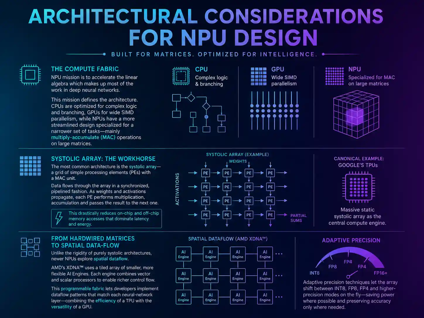
Where CPUs optimise for branching and GPUs for wide SIMD parallelism, an NPU streamlines around multiply-accumulate on large matrices — realised as a systolic array (Google TPU) or a tiled spatial-dataflow fabric (AMD XDNA™).
The compute fabric
An NPU's architecture is fundamentally defined by its mission: accelerate the linear algebra that constitutes the majority of work in deep neural networks. Where CPUs prioritise complex logic and branching, and GPUs offer broad SIMD parallelism, NPUs streamline their design to excel at a narrower set of tasks — primarily multiply-accumulate (MAC) operations on large matrices[5].
The most influential pattern for this purpose is the systolic array: a grid of simple processing elements, each containing a MAC unit, arranged so that data flows through the array in a synchronised, pipelined fashion. As weights and activations stream through the grid, each PE multiplies, accumulates, and propagates the result onward — drastically reducing the on-chip and off-chip memory accesses that dominate latency and energy[6]. Google's TPUs are the canonical example, leveraging a massive static systolic array as their central compute engine[7].
From rigid arrays to spatial dataflow
In response to the inflexibility of purely systolic designs, newer NPUs are exploring spatial dataflow. AMD's XDNA™ is the prime example: instead of a single monolithic array, it employs a tiled array of smaller, more versatile AI Engines, each combining vector and scalar processors to allow richer control flow[8]. This programmable fabric lets developers implement dataflow patterns tailored to the structure of each neural-network layer, aiming to combine TPU-level efficiency with GPU-level versatility.
At a lower level, adaptive precision techniques allow the array to shift between INT8, FP8, FP4, and higher-precision modes on the fly — saving power where possible and reserving accuracy only where needed[9].
Memory hierarchy and system integration
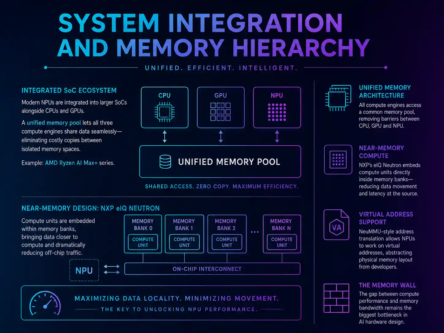
On modern accelerators, moving data — not computing on it — is what dominates energy and latency: fetching an operand from off-chip DRAM can cost far more energy than the multiply-accumulate that consumes it. That imbalance, the memory wall, is why NPU design has become as much a memory-architecture problem as a compute one[11]. A processing element that can start a MAC every cycle is idle if the memory system cannot feed it, so peak compute is only ever as useful as the bandwidth behind it.
Three techniques attack the problem at different distances from the data. A unified memory pool — shared by the CPU, GPU, and NPU on a single SoC, as in AMD's Ryzen AI Max+ series — removes the copies that isolated memory spaces force between engines, enabling near-zero-copy hand-offs[10]. Near-memory compute goes further, embedding compute units inside the memory banks themselves — NXP's eIQ Neutron is one example — so operands travel a fraction of the distance. And virtual-address support (NeuMMU-style translation) lets the NPU operate on virtual addresses, abstracting physical layout from the developer while keeping data resident. Each step trims off-chip traffic; none closes the memory wall outright, which is why it remains AI hardware's defining bottleneck.
Attacking the memory wall at three distances from the data — a shared unified memory pool for zero-copy hand-offs, near-memory compute inside the banks, and virtual-address translation that keeps data resident.
The software gap
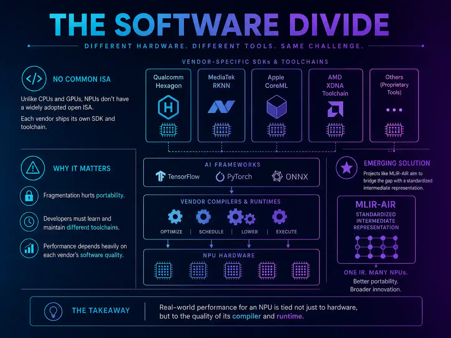
Unlike CPUs and GPUs, NPUs lack a widely adopted open ISA. Where a CPU or GPU exposes a stable instruction set that compilers have targeted for decades, each NPU vendor ships its own SDK and compiler toolchain — Qualcomm Hexagon, MediaTek RKNN, Apple CoreML, the AMD XDNA toolchain — to lower a trained model into hardware-specific code[12].
The path a model travels is the same in outline everywhere, even as the tools differ. A network authored in TensorFlow, PyTorch, or ONNX is handed to the vendor's compiler, which optimises the graph, schedules and lowers it to the device's operators, and produces a runtime that executes on the NPU. Because so much of the delivered performance is decided in that compiler and runtime rather than the silicon, two chips with identical peak throughput can behave very differently, and a model tuned for one vendor's stack often needs real rework to move to another.
That fragmentation is the field's central portability problem, and it is what emerging projects like MLIR-AIR target: an MLIR-based intermediate representation meant to map one model efficiently across many NPU fabrics, so the same program can be lowered to different vendors' hardware[13]. Either way the lesson holds — an NPU's real-world performance is inseparable from the quality of its compiler and runtime.
No common ISA: every vendor ships its own SDK and compiler, so the same framework model (TensorFlow, PyTorch, ONNX) is optimised, scheduled, lowered, and executed differently on each fabric — the gap MLIR-AIR aims to bridge.
02
Real-world applications and market penetration
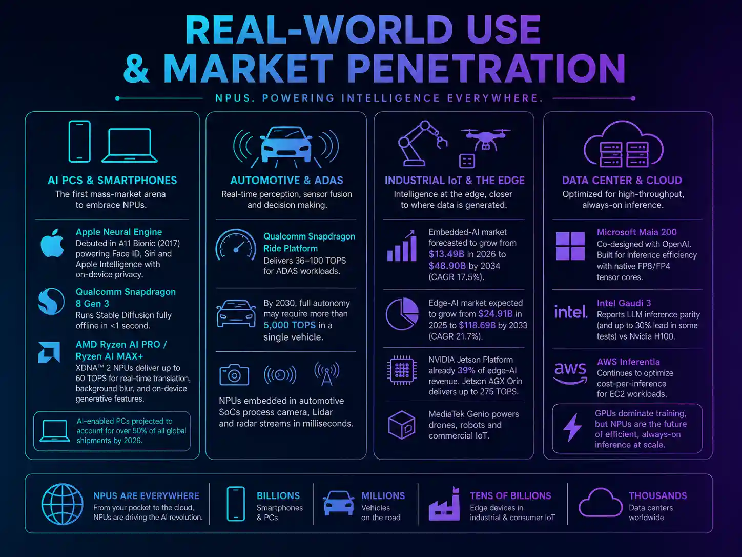
NPUs now span four arenas — smartphones and AI PCs, automotive and ADAS, industrial IoT and the edge, and always-on inference in the data center.
Smartphones and AI PCs
The smartphone was the first mass-market domain to embrace NPUs. Apple's introduction of the Neural Engine in the A11 Bionic in 2017 was the pivotal moment — accelerating Face ID, Siri, and later Apple Intelligence with on-device privacy[14]. Today, Qualcomm's Snapdragon 8 Gen 3 can run Stable Diffusion entirely offline in under a second[15]. On the PC side, AMD's Ryzen AI PRO and Ryzen AI MAX+ families integrate XDNA™ 2 NPUs offering up to 60 TOPS for real-time translation, background blur, and on-device generative features. AI-capable PCs are projected to account for more than half of global PC shipments by 2026 on several analyst forecasts.
Automotive and ADAS
Advanced driver-assistance systems require immense compute for real-time perception, sensor fusion, and decision-making. Qualcomm's Snapdragon Ride platform delivers 36–100 TOPS, and industry projections suggest a single vehicle may require more than 5,000 TOPS by 2030 to enable full autonomy[16]. NPUs are embedded directly into automotive SoCs to process camera, LiDAR, and radar streams in milliseconds.
Industrial IoT and the edge
The embedded-AI market is forecast to grow from $13.49 B in 2026 to $48.90 B by 2034 (CAGR 17.5%), and the broader Edge-AI market from $24.91 B in 2025 to $118.69 B by 2033 (CAGR 21.7%)[17]. NVIDIA's Jetson platform already captures 39% of edge-AI revenue, with the Jetson AGX Orin module delivering up to 275 TOPS. MediaTek's Genio targets drones, robots, and commercial IoT.
Cloud and data center
GPUs still dominate training, but their power draw is a liability for always-on inference. Microsoft's Maia 200, co-designed with OpenAI, is explicitly positioned for inference efficiency with native FP8/FP4 tensor cores[18]. Intel's Gaudi 3 has reported LLM-inference parity (and in some tests, up to a 30% lead) versus NVIDIA's H100, while AWS Inferentia continues to optimise cost-per-inference inside EC2[19].
35–70%
Power reduction reported by NPU-based servers versus equivalent GPU inference workloads, while matching or exceeding throughput.[20]
03
Comparative analysis: GPU vs TPU vs NPU
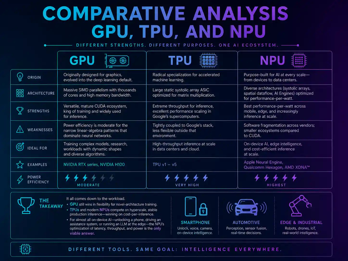
Different strengths for different jobs: the GPU's versatile CUDA ecosystem, the TPU's systolic-array throughput, and the NPU's performance-per-watt across mobile, edge, and increasingly inference at scale.
GPUs — originally built for graphics — became the deep-learning default thanks to massive SIMD parallelism and the maturity of CUDA. Their strength is versatility and ecosystem; their weakness is power efficiency for the narrow linear-algebra patterns that dominate neural networks.
TPUs represent radical specialisation. A custom ASIC organised around a large static systolic array, the TPU excels at high-throughput matrix multiplication — particularly inference — and scales effectively within Google's supercomputers. The trade-off is tight coupling to Google's stack and reduced flexibility outside that environment[21].
NPUs occupy the middle ground, defined less by a single architecture than by a focus on performance-per-watt inside SoCs. In one published evaluation, NPU-based inference servers matched or exceeded GPU throughput while drawing 35–70% less power — though the exact figures depend heavily on model, precision, and batch size[20]. Modern designs like XDNA™ further blur the line, offering tiled, programmable AI Engines that approach GPU-style flexibility without surrendering much NPU efficiency.
GPU
Versatile SIMD, mature CUDA ecosystem, dominant for training and broad inference. Moderate power efficiency. Examples: NVIDIA H100, RTX series.
TPU
Specialised systolic-array ASIC. Peak efficiency on matrix ops, tightly coupled to Google's stack. Examples: TPU v1–v5.
NPU
SoC-integrated, optimised for performance-per-watt across mobile, edge, and increasingly inference at scale. Examples: Apple Neural Engine, AMD XDNA, Qualcomm Hexagon.
Ultimately, the choice is workload-driven. For novel-architecture training, the GPU still wins on flexibility. For hyperscale, stable production inference, TPUs and modern NPUs compete on cost-per-inference. For nearly all on-device AI — unlocking a phone, driving an assistance system, running an LLM at the edge — the NPU's joint optimisation of latency, throughput, and power is usually the most practical answer.
04
Metrics, benchmarks, and emerging trends
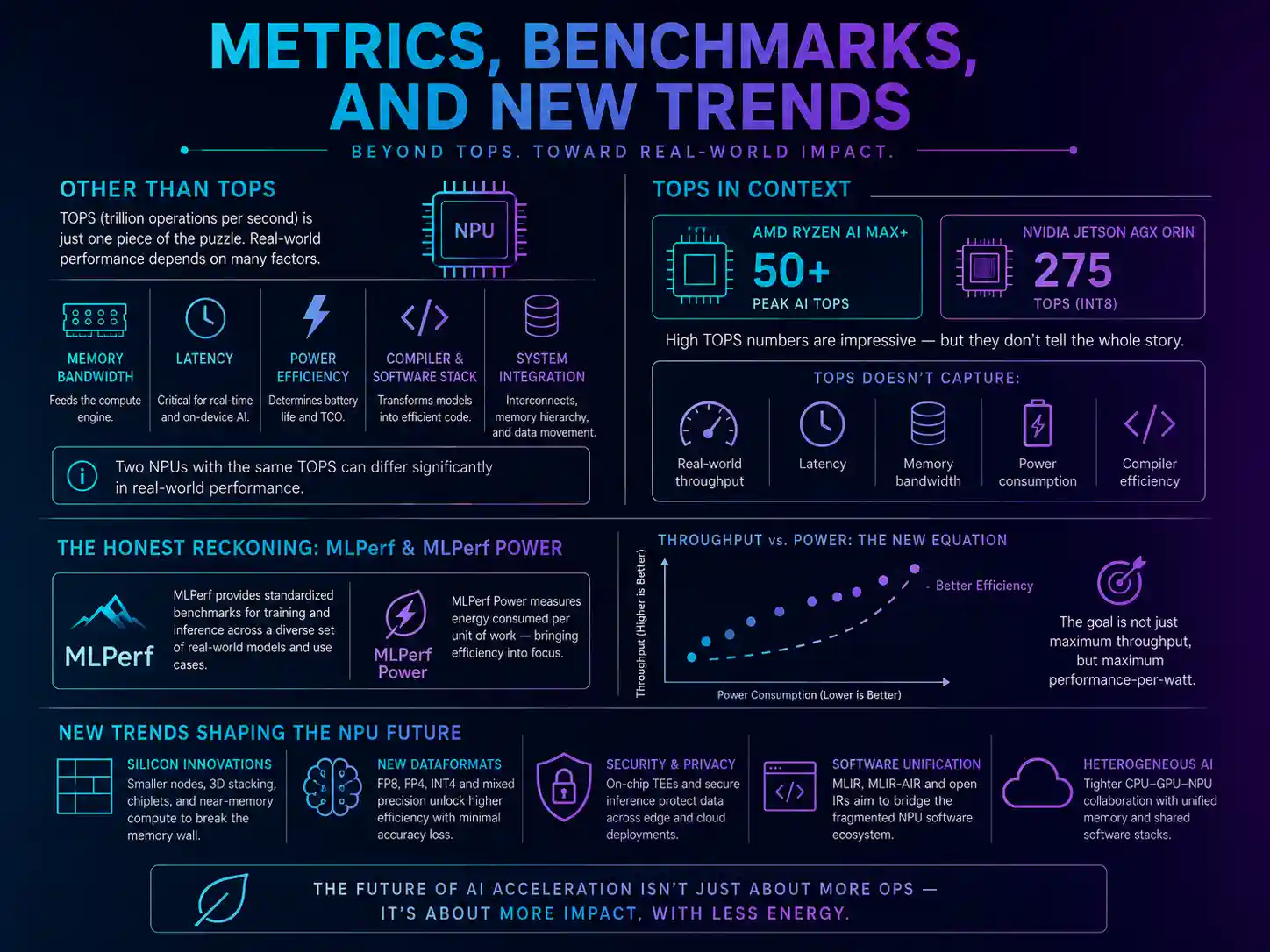
TOPS is one number among many. Real-world performance also turns on memory bandwidth, latency, power, and compiler quality — which is what MLPerf and MLPerf Power are built to measure.
Beyond TOPS
TOPS (trillion operations per second) is the most quoted NPU metric — AMD's Ryzen AI MAX+ 395 advertises 50+ peak AI TOPS; NVIDIA's Jetson AGX Orin reaches 275 TOPS at INT8[22]. It is also one of the least informative figures on its own. A TOPS number is a theoretical ceiling — the product of the number of MAC units, their clock, and the lowest precision a vendor is willing to quote — measured under conditions a real workload rarely sees.
What that single number leaves out is most of what decides whether a model actually runs well:
Memory bandwidth — the rate at which operands can be fed to the compute units; a bandwidth-bound layer leaves most of those TOPS idle.
Latency — time to first and each subsequent result, which governs interactive and real-time on-device AI.
Power and thermals — sustained throughput inside a battery or fanless enclosure, not a burst figure on a bench.
Compiler and runtime efficiency — how much of the theoretical peak the software stack can actually reach for a given model.
Numeric precision — a part rated at 275 INT8 TOPS may deliver a fraction of that at the FP16 some models still need.
Because of all this, two NPUs quoting identical TOPS can differ several-fold on the same workload, which is why peak TOPS is best read as a rough upper bound rather than a performance promise.
The honest reckoning comes from MLPerf — standardised training and inference benchmarks across representative models — and from MLPerf Power, which reports energy consumed per unit of work[23]. As data-center electricity costs rise and sustainability metrics tighten, performance-per-watt on real workloads is becoming as important as peak throughput.
What's next
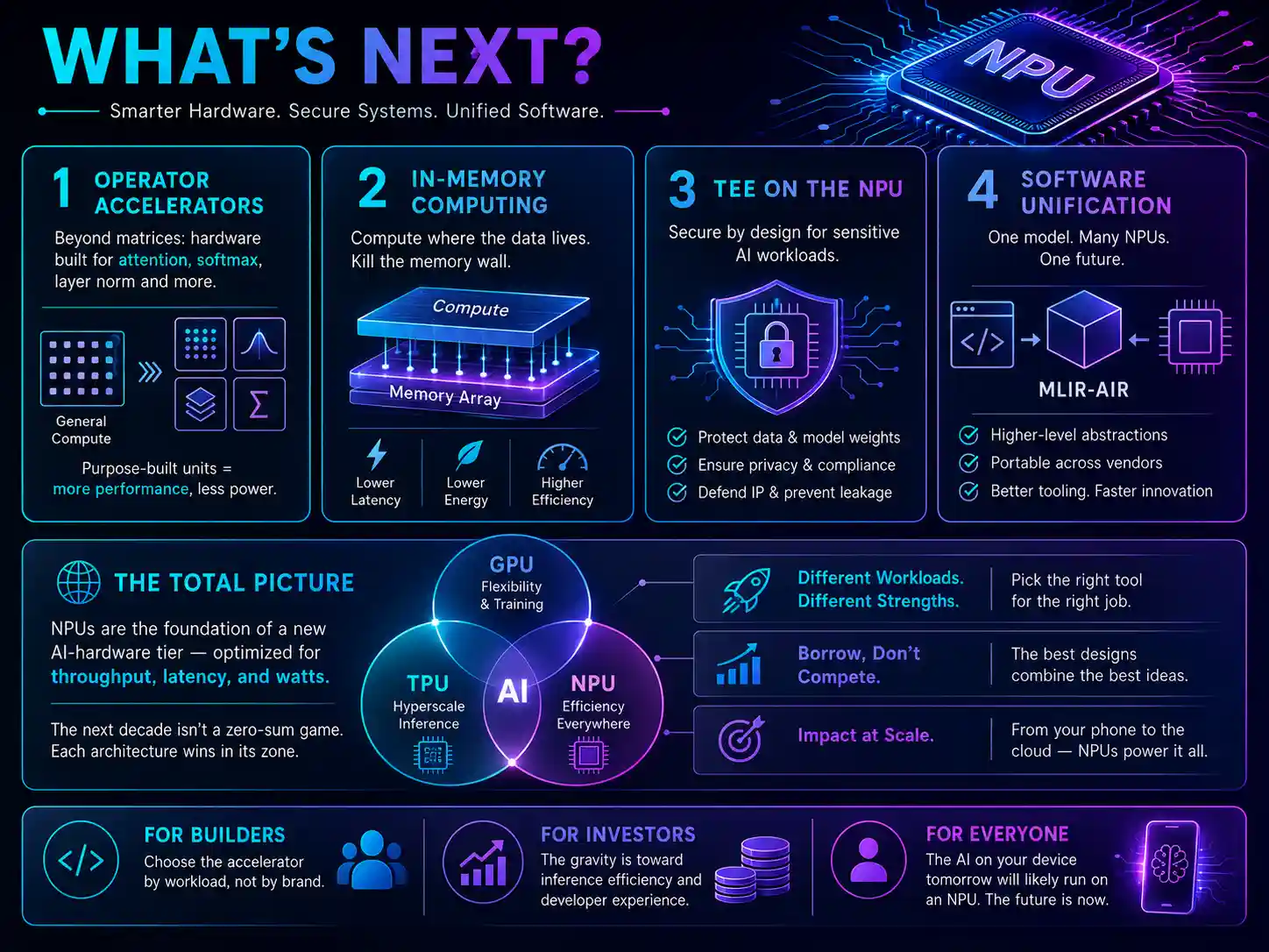
Dedicated operator accelerators. Most NPUs are optimised for dense matrix multiplication, but transformer-era workloads spend significant time in attention and softmax. Specialised hardware for these specific layers is emerging as a meaningful performance lever[24].
In-memory compute. Performing operations directly inside memory arrays attacks the memory wall head-on. Eliminating data movement promises substantial latency and energy gains for next-generation accelerators.
Trusted execution environments (TEEs) on the NPU. As AI handles increasingly sensitive data, isolating computation and model weights inside protected hardware regions becomes essential for privacy, IP protection, and regulatory compliance.
Software unification. The lack of a universal NPU ISA remains the field's biggest friction point. Higher-level abstractions like MLIR-AIR are the most promising path toward a portable NPU programming model, and any vendor that ships truly developer-friendly tooling stands to gain disproportionate market share.
The near-term roadmap — operator accelerators for attention and softmax, in-memory compute against the memory wall, on-chip trusted execution environments, and software unification through a shared IR.
·
The bigger picture
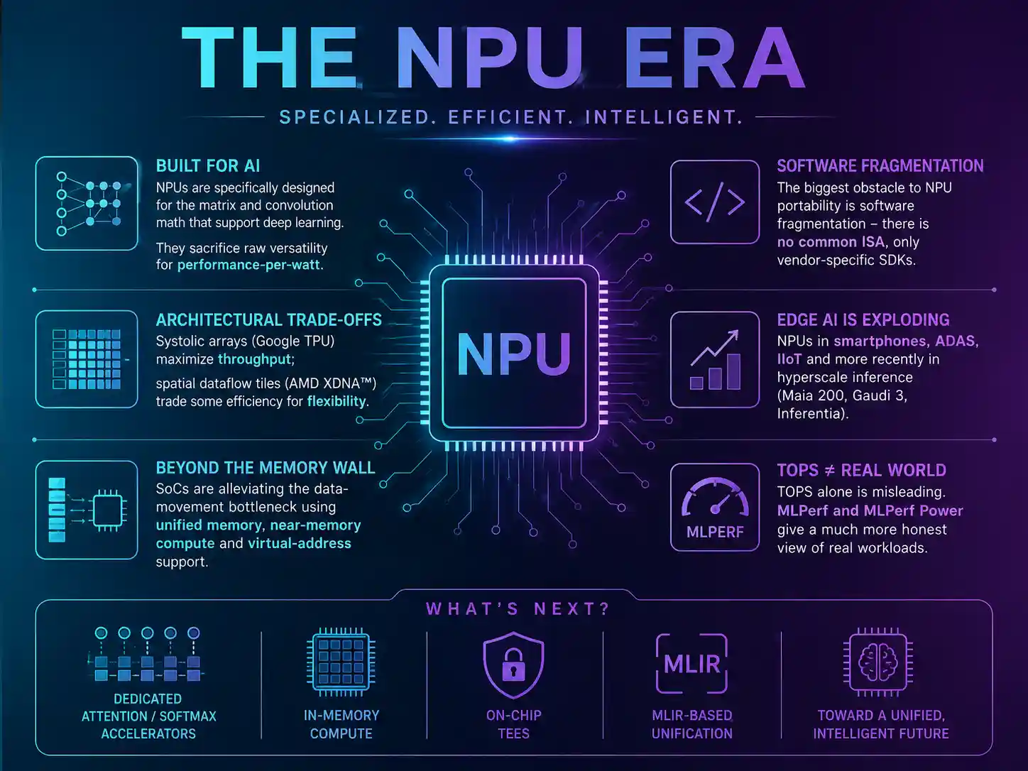
The NPU era in one frame — purpose-built silicon, architectural trade-offs, the memory wall, software fragmentation, and the shift from peak TOPS to honest, workload-level benchmarking.
NPUs are no longer a niche mobile accelerator — they are the foundation of an AI-hardware tier defined by joint optimisation of throughput, latency, and watts. The next decade will not be a GPU-vs-TPU-vs-NPU zero-sum battle; each architecture serves a distinct workload zone, and the most interesting designs are the ones that borrow from all three.
For builders: pick the accelerator by workload, not by brand. For investors: the gravity is moving toward inference efficiency and developer experience. For everyone else: the AI you use on-device tomorrow will almost certainly be running on an NPU — and the architectural choices made today will shape what that experience feels like.
Maia 200: The AI accelerator built for inference. Microsoft Blog. blogs.microsoft.com
AI Accelerators for Large Language Model Inference. arXiv 2506.00008. arxiv.org
Unlocking the AMD Neural Processing Unit for ML Training. arXiv 2504.03083. arxiv.org
A Survey on Deep Learning Hardware Accelerators. arXiv 2306.15552. arxiv.org
Exploring Edge AI Performance with NVIDIA Jetson Orin NX. Dell Community.
Benchmarking TPU, GPU, and CPU Platforms for Deep Learning. arXiv 1907.10701. ar5iv.labs.arxiv.org
Lightweight and Energy-Efficient Deep Learning Accelerator for Real-Time Object Detection on Edge Devices. ResearchGate.
We value your privacy
We use cookies to enhance your browsing experience, analyze site traffic, and personalize content. Essential cookies are always on. You can accept all, reject non-essential, or customize your choices.
Cookie Policy
Privacy Preferences
Choose which categories of cookies and tracking you allow. You can change these settings at any time from the footer.
Strictly Necessary Always Active
Required for the site to function — page navigation, secure areas, and remembering your consent choice. Cannot be disabled.
Analytics & Performance
Anonymous Google Analytics data so we can understand how the site is used and improve it. No personal identifiers are stored.
Functional
Remembers preferences such as language and region to give a more personalized experience on return visits.
Marketing & Personalization
Used to measure ad effectiveness and show content relevant to your interests. Linked to the CCPA "Do Not Sell or Share" right — disable this to opt out.